Help | Search Robot | Login

Semiconductor Devices

Remaining Time: Unlimited

Semiconductor Devices

Semiconductor technology, propelled by the transistor, has revolutionized computing, information technology, and mobile devices. Breakthroughs by researchers like Shockley, Bardeen, and Brattain led to the first transistor and subsequent advancements. Atalla's surface process improved transistor performance and popularized silicon. Atalla and Kahng's MOSFET enabled miniaturization for high-density integrated circuits. Sah and Wanlass developed the dominant MOSFET fabrication method for microprocessors.

These innovations yielded smaller, efficient devices, transforming spaceflight, wristwatches, radios, and paving the way for pocket-sized smartphones. Silicon semiconductors shaped the electronics landscape, leading to the renaming of the region as Silicon Valley.


Try it Out:


a. A   is a semiconductor device made by sandwiching a layer of n- or p-type semiconductor material between two layers of p- or n-type semiconductor material respectively.


b. What is the primary material used in the majority of semiconductors?

Diodes

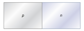
Perhaps the simplest device that can be created with a semiconductor is a diode. A diode is a circuit element that allows electric current to flow in only one direction, like a one-way valve (see Model of Conduction in Metals). A diode is created by joining a p-type semiconductor with an n-type semiconductor. The junction between these materials is called a p-n junction. 

A comparison of the energy bands of a silicon-based diode is shown in the figure below.
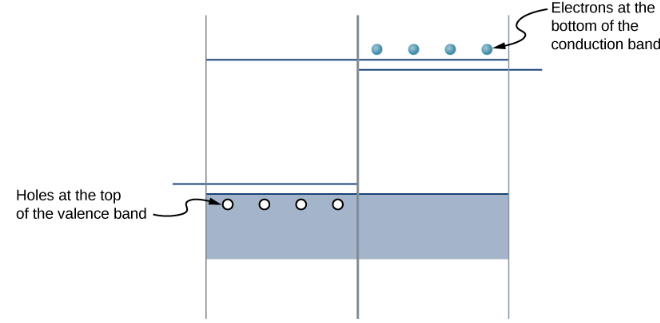
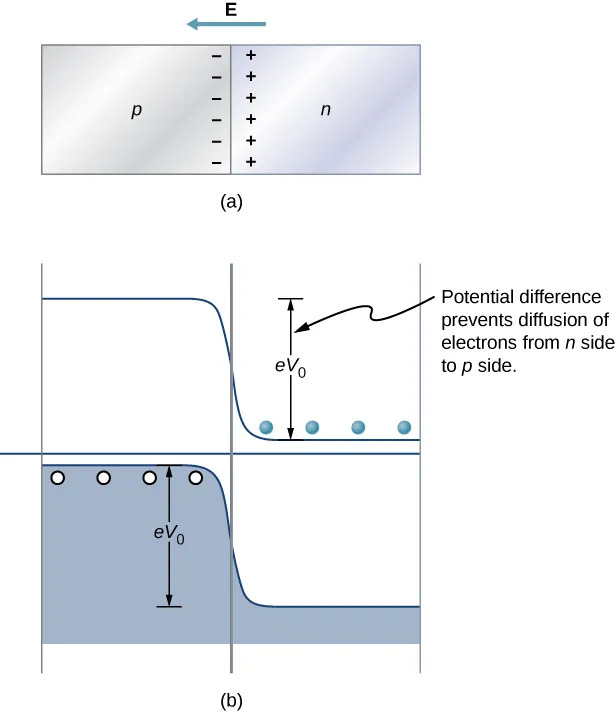


In a pn junction, the valence and conduction bands have the same positions, but the impurity levels differ. Electrons from the conduction band of the n-type material move to the p-side, combining with holes in the valence band. This results in positive ionized donor ions on the n-side and negative ionized acceptor ions on the p-side. The accumulation of charge forms a narrow depletion layer at the pn junction. The electric field associated with this layer prevents additional diffusion. The potential energy for electrons across the pn junction is represented by the figure below.


A semiconductor diode behaves differently based on its bias configuration. When the positive side of the battery is connected to the n-type material, the depletion layer widens, increasing the potential energy difference across the p-n junction. This inhibits electron movement, resulting in significantly reduced current. This is known as the reverse bias configuration. Conversely, when the positive side of the battery is connected to the p-type material, the depletion layer narrows, reducing the potential energy difference. This allows electrons to flow easily, known as the forward bias configuration. Overall, the diode enables current to flow in one direction while blocking it in the opposite direction, functioning as a one-way valve.


Try It Out:


Effect of forward biasing on the depletion layer is   

Step-By-Step Mathematical Derivation


Let's find the equation net current:


Step 1: We start by considering an n-type material with  N  negatively charged majority carriers (electrons donated by impurity atoms) and a pn junction with a potential barrier V across it.


Section


Try it out:


Select the region that depicts the reverse bias configuration in the given Current versus voltage across a p-n junction (diode).


Try it Out:


Attaching the positive end of a battery to the p-side and the negative end to the n-side of a semiconductor diode produces a current of 4.4×101A. The reverse saturation current is 2×10⁵A. (The reverse saturation current is the current of a diode in a reverse bias configuration such as this.) The battery voltage is 0.2V. What is the diode temperature?


Build Number : f3dc67a